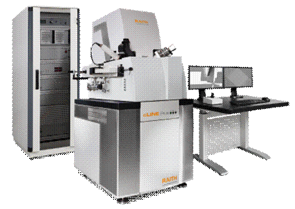
1. Instrument Name: Electron Beam lithograph (EBL)
Model: e-Line plus
Manufacturer: Raith
2. The mainfunctionof the instrument
eLINE Plus is a high-performance electron beam exposure (EBL) system that can simultaneously apply multiple nano-processing technologies. It have the smallest electron beam spot (<1.6nm) in the world, and the smallest processing line width, 8nm. eLINE Plus uses advanced electron beam exposure technologies, including high-precision laser interference sample stage, high-speed and high-precision pattern generator, pattern recognition automatic engraving, which can simultaneously meet the requirements of ultra-high resolution and large-area micro-nano processing.
3. Main Specifications
The minimum processing line width: 7 nm
The electron beam photoresist: PMMA 950K A4 (positive)
EHT: 10kV, 20kV; Aperture: 7μm, 20μm, 30μm
4. Sample requirements (if any)
Conductive substrate.

